New techniques for interconnecting and stacking transistors should make it possible to push the density and precision of processors even further.
Fifty years ago, in 1971, Intel marketed its first microprocessor, the 4004, which consisted of 2,250 transistors. The 8086, the first American 16-bit processor, had 29,000 transistors, then 275,000 on the 80386 and even 1,180,235 transistors on the 80486 before the Pentium revolution and its 3,100,000 transistors. Impressive figures for the 70s, 80s and 90s, but which now seem quite paltry when Intel advances the number of 3 200 000 000 on the Core i7 Broadwell of 2016. Today, the American company no longer communicates this kind of figures, but continues its work in order to "still fit".
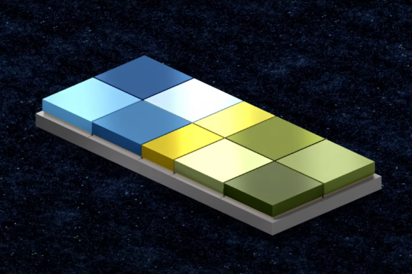
On the occasion of the 67e edition of the IDEM or International Electron Devices Meetingintel presented several advances to show us what it envisions for the future of its processors. In the video above, Marko Radosavljevic, a senior engineer at Intel, goes into detail about the different stacking techniques associated with various substrates used by the American company in order to multiply the density within its chips. In particular, 3D CMOS, whose 30 to 50% increase in stacking compared to current techniques, should make it possible to group more and more transistors per square millimeter.
Currently, Intel operates the process of engraving Intel 7 on the processors of Alder Lake generation. Later on, it plans to switch to Intel 4 and Intel 3. These changes will be made possible by using Foveros Direct packaging instead of Foveros. The objective here is the multiplication of interconnections in order, of course, to maximize the exchanges. Intel has already talked about these improvements, notably at theIntel Accelerated conference last July.Foveros Direct uses "copper-to-copper" connections, which have been miniaturized compared to Foveros, so that the number of interconnections in a given space is drastically higher, and more interconnections mean more exchanges between the different parts of the chiplets. Intel also points out that Foveros Direct also allows for greater design modularity. All this is summarized in three words, theHybrid Bonding Interconnect,or HBI.
Finally, at this 67e edition of IDEM, Intel also talked about replacing the so-called FinFET transistors (field-effect transistor or finned field effect transistor). As Samsung or TSMC can also consider, Intel will move to GAA FET (gate-all-around) a technique that aims to modify the structure of the transistor so that more channels are implemented. In this case, the aim is to increase the precision and, above all, the stability of the transistors, an essential subject as soon as the engraving process is refined again and again. However, the introduction of GAA FET transistors at Intel is not expected before 2024 and the use of the Intel 20A process.


