Naming its engraving nodes differently to take into account the density of transistors.
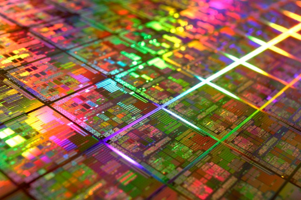
It's no secret for anyone who follows semiconductor news closely or remotely, if Intel remains a giant in the sector it is also in great difficulty with certain technical processes. For several years now, it seems to have all the difficulties of the world to make evolve its process of engraving of components towards 10 nm and 7 nm whereas one of its main competitors - the Taiwanese TSMC - already evokes the passage to 5 nm even to 4 nm and 3 nm.

In fact, while AMD - TSMC's partner - has been able to market its new Ryzen 5000 series using the 7 nm process, Intel has just distributed its new Rocket Lake-S range using a 14 nm process: from a strict marketing point of view, this is not a very good idea. Intel is therefore considering rethinking the way it names its etching process, and no longer reflects the etching fineness alone, but also takes into account the density of transistors per square millimeter. This is certainly a marketing maneuver, but not only.
It is important to know that not all etching processes are equal. There is no "standard" in this field to refer to this or that process, its finesse and its quality. Intel emphasizes that its 10nm process is much more efficient than TSMC's 7nm process: 10nm allows the American company to achieve a transistor density of 100.8 million transistors per square millimeter (MT/mm²), while the Taiwanese company has to be satisfied with 90 MT/mm² on its 7nm process. According to Oregon Live, the idea of revising the entire nomenclature and advocating for something more universal is gaining ground at Intel.


