Connection to DriversCloudCreate a DriversCloud.com accountReset your DriversCloud.com passwordAccount migration
A confession of impotence or a legitimate readjustment? Samsung renames its most modern engraving node
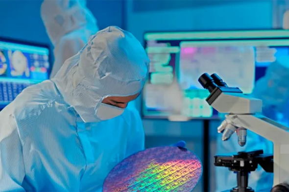
10 nm, 7 nm, 4 nm... The three semiconductor giants are battling it out over nanometers.
Former number one in semiconductor manufacturing, American company Intel has experienced a number of setbacks in its management of 10 nm technology, a particularly fine etching process that represented the Holy Grail just a few years ago. No doubt as a direct consequence of the problems encountered with 10 nm, Intel has decided to revise the way it names the etching nodes it uses. Thus, in July 2021, the American company abandoned nanometer names and " 10 nm " became, with a wave of the magic wand, " Intel 7 ", or a way of saying " our etching process is equivalent to our competitors' 7 nm ". In reality, however, it's a 10 nm node. So why the change?
It's true that Intel has struggled with 10 nm, but to its credit, the American company is capable - at the same etch level - of a much higher transistor density than its competitors. In fact, when Intel engraves in 10 nm, the chips it produces are capable of integrating far more transistors than those of Taiwanese manufacturer TSMC or South Korean Samsung, its two main competitors. The name change introduced by Intel almost three years ago served a dual purpose: to emphasize the engraving quality of Intel's processes, while at the same time bringing the company up to the level of its competitors, at least in terms of the names used.
Today, it seems that Samsung is more or less forced to do the same. More or less, because for the time being, it's only a question of renaming a single burn-in node, and even then, the matter has not been made official by Samsung Foundry, but merely mentioned by TechPowerUp, citing ZDNet Korea. According to the latter, Samsung has decided to change the name of its most modern etching process, the second-generation SF3 node. This node, although etched in 3nm, would therefore be renamed SF2. A way of saying, as Intel does, " our process is equivalent to 2 nm ". The fact remains that such a change of name has forced Samsung to review all contracts already signed, and proves if proof were needed that Intel's renewed vigour is not without its problems: by insisting on the "2" in SF2, Samsung no doubt wishes to overshadow the Intel 20A process (2 nm equivalent) which the American firm is due to launch before the end of the year. The battle between the three semiconductor giants has only just begun.
